| Характеристики | Возможности | Шаблоны |
|---|---|---|
| Слои печатной платы | до 18 слоев | / |
| Материалы подложки | FR-3, FR-4, FR-5, CEM-1, CEM-3, RCC, металл, керамика, термопластик | / |
| Мин. Размер печатной платы | 10*10mm | 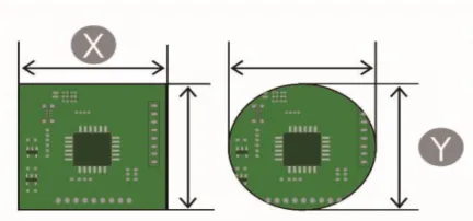 |
| Макс. Размер печатной платы | двухсторонняя: 570*1200мм Четырехслойная: 570*850 мм, шесть слоев и выше: 570*670mm |
|
| Допуск размера печатной платы | ±0,2-0,3 мм(зависит от размера печатной платы) | / |
| Толщина печатной платы | стандарт: 0,8 мм-2,0 мм нестандарт: 0,3 мм-5,0 мм | 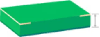 |
| Допуск толщины печатной платы | ± 0,1-0,25 мм Толщина печатной платы ≥3 мм, допуск составляет ±10%. |
/ |
| Мин. Размер площадки BGA | 7mil |  |
| Толщина наружного слоя меди | 0.5-5 OZ |  |
| Толщина меди внутреннего слоя | 0.5-2 OZ | 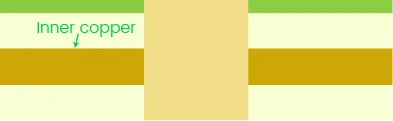 |
| Минимальная ширина линии | 4mil | 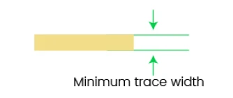 |
| Минимальное расстояние между линиями внешнего слоя | 4mil - 7mil | 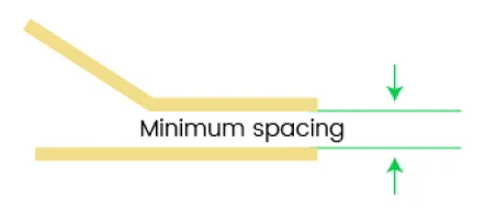 |
| Минимальное расстояние между линиями внутреннего слоя | 4mil - 7mil | |
| Диаметр сквозного отверстия печатной платы | Стандарт: 0,3 мм-2,5 мм Экстремальный: 0,15 мм | 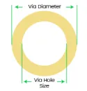 |
| Мин. Допуск сверлильного паза | Направление ширины паза: ±0,1 мм, направление длины паза: ±0,15 мм |  |
| Мин. Допуск фрезерного паза | Ширина и длина паза: ±0,15 мм | |
| Мин. Толщина меди (сквозное отверстие) | 25um | 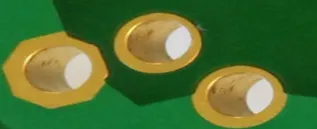 |
| Мин. Толщина слоя меди (заглубленные/слепые отверстия) | 20um | 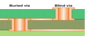 |
| Прочность отслаивания жесткого флекса | ≥1.4N | / |
| Обработка поверхности колодки | HASL, ENIG, OSP, ENEPIG, I-Ag, I-Sn | / |
| Толщина золотого покрытия | 0.25-1.3um | 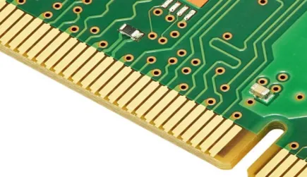 |
| Золото палец никель толщина покрытия | 3-5um | |
| Цвет паяльной маски | Зеленый, красный, желтый, синий, белый, черный, фиолетовый | 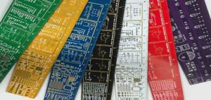 |
| Мин. Толщина паяльной маски | 10um |  |
Your Cart
Ваш надежный производитель печатных плат с 2006 года, предлагающий услуги по производству, сборке и проектированию.
- devin@yongve.com
- 4F, Building 2, Guanghui Technology Park, Mingqing Rd, Longhua, Shenzhen, China
Продукция и услуги
- Многослойная печатная плата
- Тяжелая медная печатная плата
- Алюминиевая печатная плата
- Быстрый поворот печатной платы
- Прототип печатной платы
- Сборка печатных плат под ключ
Возможности
Ресурсы
- Блог
- Отзывы клиентов
- Техническая поддержка
- Онлайн просмотрщик гербер
Сертификация
Варианты доставки
Способы оплаты
Свяжите нас с нами на
Copyright © 2026YONGVE : производитель печатных плат и печатных плат