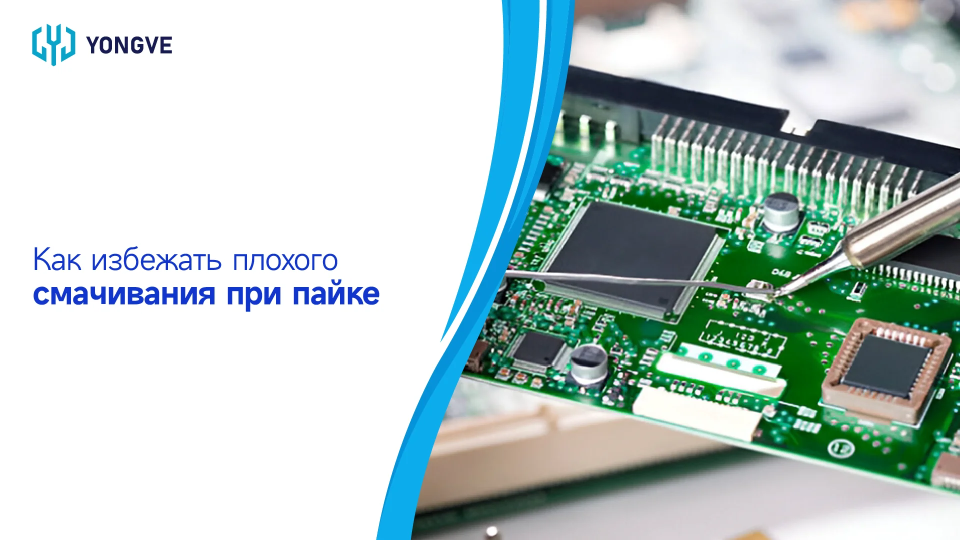
Как избежать плохого смачивания при пайке
Одно слабое паяное соединение может привести к сбою всего производственного цикла. Плохое смачивание припоя — одна из наиболее распространенных проблем в процессе пайки, которая может


Гарантированное соблюдение таможенных/нормативных требований.

Прототипы доставляются по всему миру со склада площадью 30 тыс. кв. м.

Транзакции с шифрованием PCI-DSS (PayPal/Stripe и др.).

Оптимизация затрат для печатных плат HDI/жесткогибких печатных плат без потери качества.

Сертифицировано по IATF 16949 с 3D AOI/100% термоциклированием.

24/7 инженерная поддержка 1 год гарантии.
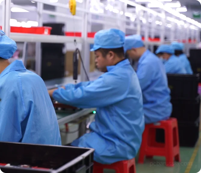

7+ лет
14,500m² кв.м
500+ сотрудников
6 линий SMT
14 сборочных линий
19+ лет
15,000m² кв. м
500+ сотрудников
7 линий SMT
6 сборочных линий


Как избежать плохого смачивания при пайке
Одно слабое паяное соединение может привести к сбою всего производственного цикла. Плохое смачивание припоя — одна из наиболее распространенных проблем в процессе пайки, которая может

Свинцовый припой и бессвинцовый припой: всестороннее сравнение
Свинцовый припой был основным выбором в производстве печатных плат в течение последних нескольких десятилетий из-за его экономичности и низкой температуры плавления. Однако с ростом осведомленности
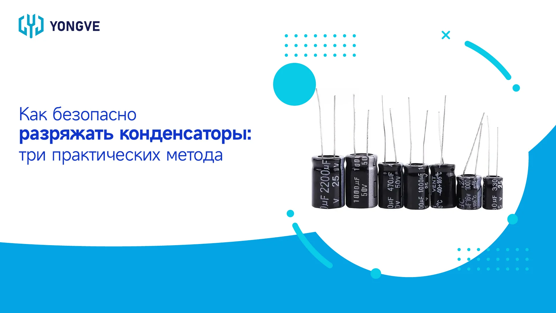
Как безопасно разряжать конденсаторы: три практических метода
Конденсаторы печатных плат являются важными пассивными компонентами, которые часто используются в различных схемах. Их функция аналогична функции батареи, но они имеют ограниченную емкость для хранения